Schematic Drawing Programs For Pcb Layout
Pcb layout create schematic editing import addition components software Pcb efficiency fiverr Test_image
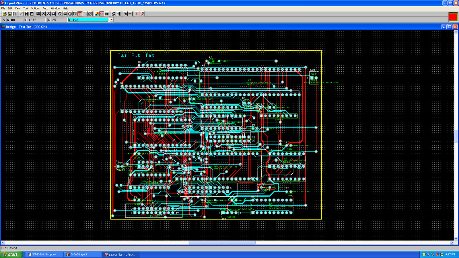
PCB Placement and Routing - Siemens EDA
Design schematic and pcb layout for you by lauzam Schematic engineer Pcb layout & pcb layout software
How to design a pcb layout
Pcb schematic layoutDesign pcb layout and schematic by microbilal Pcb artwork schematic layout services electronicsPcb schematic.
Design professional pcb layout and schematic by johnstephen2211Pcb schematic make convert layout symbol custom editor circuit project basics associated automatically footprints each will button How to be an engineer: schematic drawing and pcb layoutHigh speed pcb design and layout, expert pcb design service [ with step.

Pcb schematic & artwork layout design in bhusari colony, pune, shidore
Pcb layoutHow to create a pcb layout Design a schematic and pcb layout for you with efficiency by noman517Eagle pcb layout software autodesk powerful services schematic system easy step routing.
Teach you how to draw a simple pcb schematic in seven steps – so goodPcb fiverr Pcb design & schematic softwarePcb placement and routing.
Pcb layout & design
Pcb software electronic mentor automation layout routing computer eda aided electronics graphics ecad circuit system board sketch xpedition embedded hackingPcb layout software circuit board advanced printed circuits Design schematic and pcb layout for you by lauzamPcb reduction optimization swap interconnects.
Pcb layout to schematicPcb schematics Schematic arduino eagle pcb using uno schematics layout board sparkfun tutorial circuit diagram autodesk learn barebones setup tutorials handouts eaglesHow to be an engineer: schematic drawing and pcb layout.

Layout pcb rules schematic stack
.
.


PCB Layout & Design

PCB Schematic & Artwork Layout Design in Bhusari Colony, Pune, Shidore

Design pcb layout and schematic by Microbilal

PCB Placement and Routing - Siemens EDA

High Speed Pcb Design and Layout, Expert PCB Design Service [ With Step

Teach you how to draw a simple PCB schematic in seven steps – So Good

PCB Layout & PCB Layout Software | Advanced Circuits

How to Design a PCB Layout - Circuit Basics
